
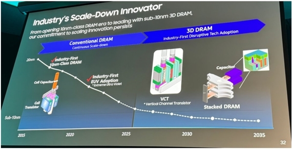
快科技4月4日消息,3D晶体管正在各种类型芯片中铺开,3D DRAM内存也讨论了很多年,但一直没有落地。如今三星公开的路线图上,终于出现了3D DRAM。
三星的DRAM芯片制造工艺目前处于1b,后续还有1c、1d,都是10nm级别。
再往后的10nm以下节点,将分别命名为0a、0b、0c、0d,其中打头的0a工艺预计2027年底-2028年初量产(月产能超过2万块晶圆),0d则要到2032年。
就在进入10nm之后,三星将全面开启3D内存时代,首先引入VCT(垂直通道晶体管),看起来应该是基础的FinFET类型,而非更先进的GAA。
大约2030-2031年的时候,三星将升级到堆叠DRAM,将多组VCT堆在一起,从而获得更大容量、更高性能,看起来还会引入电容器作为辅助。
文章来源于互联网:凤凰网-三星谋划3D堆叠内存:10nm以下一路奔向2032年
相关推荐
-
苹果充电口即将成为历史,新技术将改变充电方式
欧盟委员会宣布,从 2024 年起,USB Type-C 接口将成为欧盟电子设备的通用标准,而到 2026 年,此规定也将适用于笔记本电脑。 也就是说,USB Type-C 接口将…
-
三星Galaxy Buds3 Pro耳机真机现身:银灰色金属质感,7月10日发布
IT之家 7 月 5 日消息,博主 @i冰宇宙今日分享了一组三星 Galaxy Buds3 Pro 耳机的真机照片,大家一睹为快。 正如此前曝光渲染图所示,Galaxy Buds3…
-
富士通Quaderno彩色电子墨水屏阅读器登场:A4、A5 尺寸,学习办公新利器
IT之家 11 月 21 日消息,富士通(fujitsu)于 11 月 19 日发布博文,推出了 A4 尺寸的 QUADERNO A4 (Gen.3C)、A5 尺寸的 QUADER…
-
华硕谈AI PC:2024年开始发酵 但还有一段学习曲线
集微网消息,1月17日,华硕共同执行长胡书宾在谈到AI PC时表示,AI PC 2024年会开始发酵,但还是有一段学习曲线。 针对PC需求加温是否将落在今年下半年,胡书宾分析,有人…
-
苹果Apple MacBook Pro M3 Pro笔记本在美国亚马逊可以省150美元,仅售1849美元!
苹果Apple MacBook Pro M3 Pro笔记本是一款性能卓越、功能齐全的笔记本电脑,其折扣非常大,目前美国亚马逊正在开展一项优惠活动,您可以以1849美元的价格购买该产…
-
AYANEO NEXT LITE掌机预装系统由HoloISO调整为Win11家庭版
IT之家 1 月 26 日消息,AYANEO 掌机官方昨日发布公告,表示根据玩家意见将 AYANEO NEXT LITE 掌机的预装操作系统从 HoloISO(IT之家注:Holo…
-
苹果设备的新人工智能功能名称:Apple Intelligence?
苹果将于6月11日在WWDC大会上宣布其针对苹果设备的新人工智能功能集,彭博社的马克·古尔曼报道称,它的正式名称将是“Apple Intelligence”。 iOS 18、iPa…
-
摒弃安卓!华为:2024年鸿蒙生态全面进化关键一年
快科技1月1日消息,华为终端BG、首席运营官何刚更新了自己的微博,并透露了公司接下来2024年的一个重要方向。 何刚表示,刚刚过去的2023年,是不平凡的一年,也是鸿蒙原生应用的开…
-
余承东:华为MateBook X Pro比苹果MacBook Pro 14更强
凤凰网科技讯(作者/张雪雍)4月11日,华为常务董事余承东在华为鸿蒙生态春季沟通会上宣布华为MateBook X Pro正式发布。在重量和功率方面,余承东称此款产品比Apple M…
-
华为MatePad Pro13评测:超越iPad的全能平板
2010年,平板电脑在乔布斯的构想下诞生。在当时数码媒体几乎空前一致的“大号 iPhone”嘲笑声中,iPad 凭借大屏和手机交互的优势,在手机与 PC 之间开辟出了一块全新的战场…
